Know-abouts PCB surface finishing: importance and common methods
By: Frank
At EPR we design PCBs for various customers, and those boards will be used for even more applications. We design, for example, test boards with expensive sockets, PCBs with the smallest available BGA pitch (0.35mm), PCBs which are used for high temperature stress and boards that need to carry RF signals. Regardless of the board or the application, the finishing is of great importance in the design and production of a PCB. That is why this blog zooms in on the finishing on PCBs.
When a design is finalized and a layer stack is defined, a description file is enclosed that tells a PCB manufacturer what kind of finishing is requested. This surface finish is in between the components and the board’s copper. It is applied for solderability and to protect the copper layer. The type of finishing is important and is determined by the PCB usage. There are several finishing methods and the five most common will be described here.
(1) HASL = Hot Air Solder Leveling
HASL used to be the most used surface finishing, using a tin bath and remove its remains by hot air. But as the components have higher densities nowadays, a more flattened surface is needed. If not, HASL is cheap and still used for large volume production.
(2) OSP = Organic Solderability Preservative
OSP is a low cost and environmental friendly way of protection. It is a water based organic compound, which bonds with the PCB’s copper. OSP finishing is not recommended when plated through holes are used. OSP is very thin and fragile. Because of the many actions through hole processing demands, damage on the board can easily be made and will damage the protective layer. Also, a PCB with OSP finishing is harder to solder after the reflow process. Finally, OSP has a limited shelf life. At EPR we rarely see and design PCBs with OSP finishing.
(3) ENIG = Electroless Nickel Immersion Gold
ENIG is the most used finishing method. It is a double layer coating with 0.2 µm gold (Au) on 4 µm nickel (Ni). The gold protects the nickel, which gives a long shelf lifetime. One disadvantage is the so-called black pad phenomenon, as pictured below.
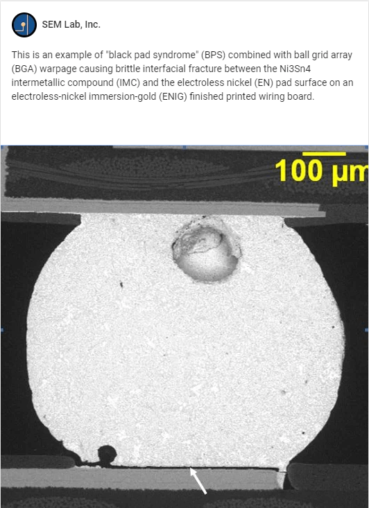
Black Pad syndrome example. Source: SEM Lab, Inc.
(4) ENEPIG = Electroless Nickel Electroless Palladium Immersion Gold
ENEPIG is a fairly new method of finishing, based on ENIG, which overcomes the black pad issue by adding a third layer of palladium (Pd). It adds an extra barrier to further reduce copper diffusion.
(5) Gold = Hard Electrolitic Gold
Hard gold finishing is used when mechanical contact pressure is opposed to the PCB. For example, PCB edge finger contacts or test sockets with pressure pins. To prevent damaging to the copper itself the surface is protected with 10 µm gold (Au) upon a nickel barrier varying from 10 to 100 µm. Its main disadvantage is its poor solderability because of the hardened golden surface. According to IPC rules, a gold thickness of 0.45 µm Au is the limit for proper soldering.
The perfect package for the perfect beating heart
When a design is finished, the layer stack is defined and the ODB++ files are generated. A final PCB description document needs to be attached to the package, which includes the best option for finishing method of the designed PCB. This best option always depends on the PCB and its application. Everything for that perfect beating heart.