
Nanotechnology in electronics: an advance towards mo(o)re
Most of us roughly know the history of electronics through the years. In the early days large components like electron tubes and paper in wax capacitors were used. This changed up to the point where we got used to integrated circuits with incredible amounts of transistors inside, stacked ceramic capacitors, flex-rigid PCBs and many other state-of-the-art components. Thanks to nanotechnology there is a lot more to come.
Nanotechnology and nanoscale
Nanotechnology is defined as the research, development and use of structures between 1 nanometer and 100 nanometers in size. A nanometer is one billionth of a meter (1 x 10⁻⁹ m), about the span of 3,5 gold atoms. To get a better understanding about the dimensions: the human hair is about 17.000-180.000 nanometers wide.
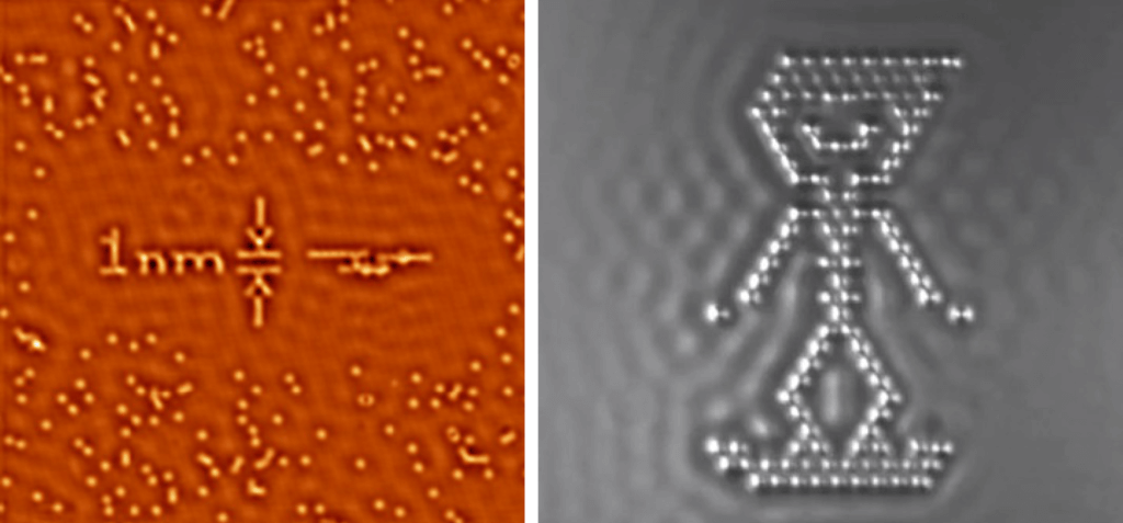
Figure 1: Oxygen atoms made visual by a scanning tunneling microscope. Source: IBM.
Nanotechnology in chips
From the moment semiconductor technology made the dense integrated circuit possible, Gordon Moore predicted that the number of transistors would double about every two years. In the early seventies, integrated circuit technology started at the micron scale. Today with structures at 7nm, physical limits to downscaling using transistors seem to be within sight. To continue Moore’s law into the next few decades, more nanotechnology is needed. Eventually another technology like photonics, that is able to process quantum information, will take the place of the current transistor technology.
Two promising nanomaterials
Graphene
Graphene is a single layer of carbon atoms arranged in a hexagonal lattice. It is 100 times stronger than steel and has excellent electrical and thermal properties. The conductivity can be altered by doping the material. In this way it could possibly replace the silicon one day. Recent discoveries show that the material can be modified into a superconductor, paving the way to even more new possibilities. Graphene is currently used to enhance existing battery technologies and it found its way into supercapacitors.
Quantum dots
Quantum dots (QDs) are crystals of a few nanometers wide made out of semiconductor material. Although consisting out of 100–100K atoms, they act as one very large atom. When energy is applied to an atom, electrons are energized and move to a higher level. When the electron returns to its lower and stable state, this additional energy is emitted as light corresponding to a particular frequency. The light frequencies of quantum dots can be precisely tuned mainly by changing the size of the dots. It is because of these properties that quantum dots are already used as a color filter in display backlights. Apart from various biological and chemical applications, there are a lot of other electronic possibilities for the quantum dots. They might even contribute to the realization of the quantum computer. The dots are also seen as a breakthrough technology in the development of more efficient solar cells, as they can break free more than one electron from one photon. The first commercial electronic component using QDs became available in 2018: a high-power white LED equipped with QDs to improve on efficiency over the conventional phosphor types.
Other electronic components already using nanotechnology
- There are ferrite toroids on the market with extremely fine-grained microstructures (grain sizes of 10 nanometers). Cores with nanocrystalline materials feature a much higher permeability (superior characteristics) compared to conventional types.
- Carbon nanotube-based electrical cables are a direct replacement for copper. The advantages: they are strong, light and non-corrosive.
- Nanowire LEDs. Nanowires are defect-free, 3D structures that enable red, green and blue micro LEDs. They have a 10 times brightness and power advantage over OLED.
The future of nanoelectronics
Future nanoelectronics are a crucial enabler of growth and competitiveness in most industrial sectors. It will enable smaller and faster components, devices will consume less energy, it will lead to better and more functional displays and higher capacity memory. The top three applications of nanotechnology are electronics, energy and biomedical. According to market researchers, they account for over 70% share of the global nanotechnology market. A market with an annual growth of 18% expected to reach approximately €150 billion by 2025.
PCB design with nanoelectronics to come
A drop-in power consumption as a result of nanotechnologies in electronic components will imply a less difficult thermal design of the PCB. The increase in operating frequency and scale integration however won’t make life easier for the designer.
A word from EPR partner
Electronics industry is probably the most interesting industry sector for the application of nanotechnology. At EPR partner we are looking forward to the new nanotechnology based electronic components to come and are happy to implement them for our customers.